Puccini "REMOTE"(up
to v4.3)
Puccini "REMOTE"(up
to v4.3)
Don't ask me why! This "philosophy" (modify a
design,
even if it works fine and people review it enthusiasticly) seems to
have
been recently applied not only to all the Puccini productions, but even
to the Paganini and Maestro CD player: they
abandoned the Sony chipset/mechanics and use a "ready to go"
Philips system.
Anyway, talking about the Puccini "remote" and the differences
with
the original, it would be worth while to review some of the circuit
diagrams.
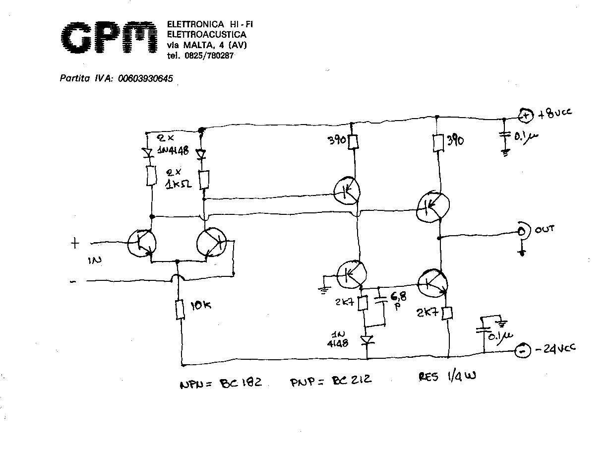
The main issue is a "discrete" operational amplifier, with an FET
differential
front-end and a transistor output stage.
Lets look at the diagram, considering that this "basic" diagram is
not always the same (i.e. some component values are different if we are
talking about the preamplifier section or the driving section):
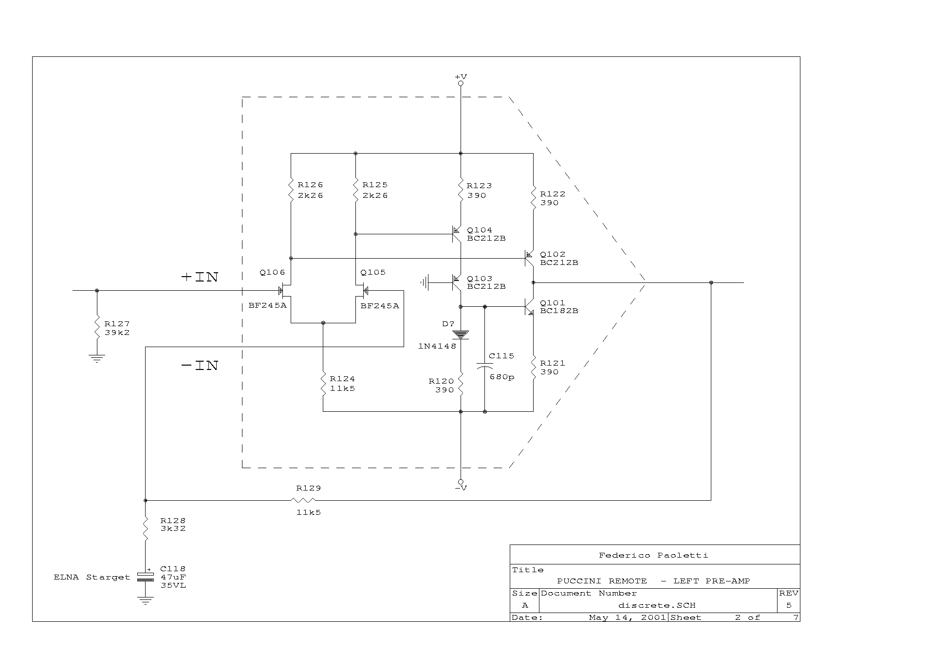 Here's
the BASIC (not the exact) diagram used in the preamplifier section (GIF
22k)
Here's
the BASIC (not the exact) diagram used in the preamplifier section (GIF
22k)
As you can see it is a "text-book" circuit; I've
seen it as a gain block (GIF 16k) on the![]() Italian Hi-Fi review (Fabrizio Montanucci, July/August 1992), as well
as
in the MONRIO MC202 power amplifier (PS
116k),
but
in both case the input was a bipolar, not an FET!
Italian Hi-Fi review (Fabrizio Montanucci, July/August 1992), as well
as
in the MONRIO MC202 power amplifier (PS
116k),
but
in both case the input was a bipolar, not an FET!
Here you see what happens if the load on the output is varied
from
near-infinite to a more realistic value: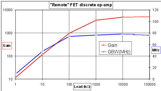
Look! Even for a light load of 47k the OL gain drop from 5000 to
500;
this is due to the "collector output", that does not isolate the load.
This happens in an asymmetrical way: in fact the output transistor
Q101 is somewhat isolated with the help of Q103, and does not "load"
the
differential stage; this is not true for the other output transistor,
Q102:
its base is directly connected to Q106's drain, presenting the output
load
to it, and so affecting the Open-Loop gain.
Another important difference is the "gain" of a differential
circuit:
bipolar gains are higher than FET's. Period!
Here you can see how Bipolar is better than FET, considering the net
gain and the Gain-Bandwidth product:
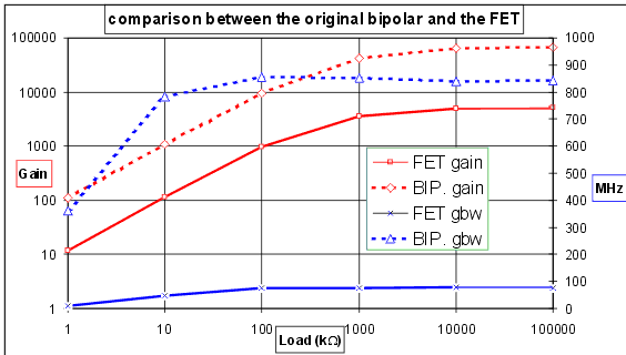
The only advantage using FET is the "near zero" input current, that
is priceless for some applications; but not in this generic audio case.
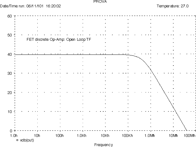
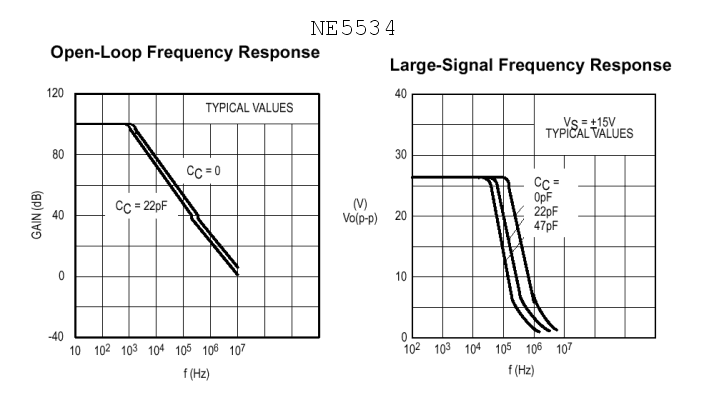
To end the analysis of this circuit, take a look at the omnipresent NE5534: as you can see the OL gain at 100kHz is still very high (something near 60dB), while the gain of the discrete FET amplifier used in the "remote" has dropped to less than 40dB when the load is less than 10k (as is in the case of the power stage, which has an input resistance of 8.3 kW):
Because the same circuit is used for driving the power output stage (you can imagine how low and non-linear the input impedance is of this), problems will be even worse. More about this later.
Up to now it's been theoretical; now let's look at practical matters.
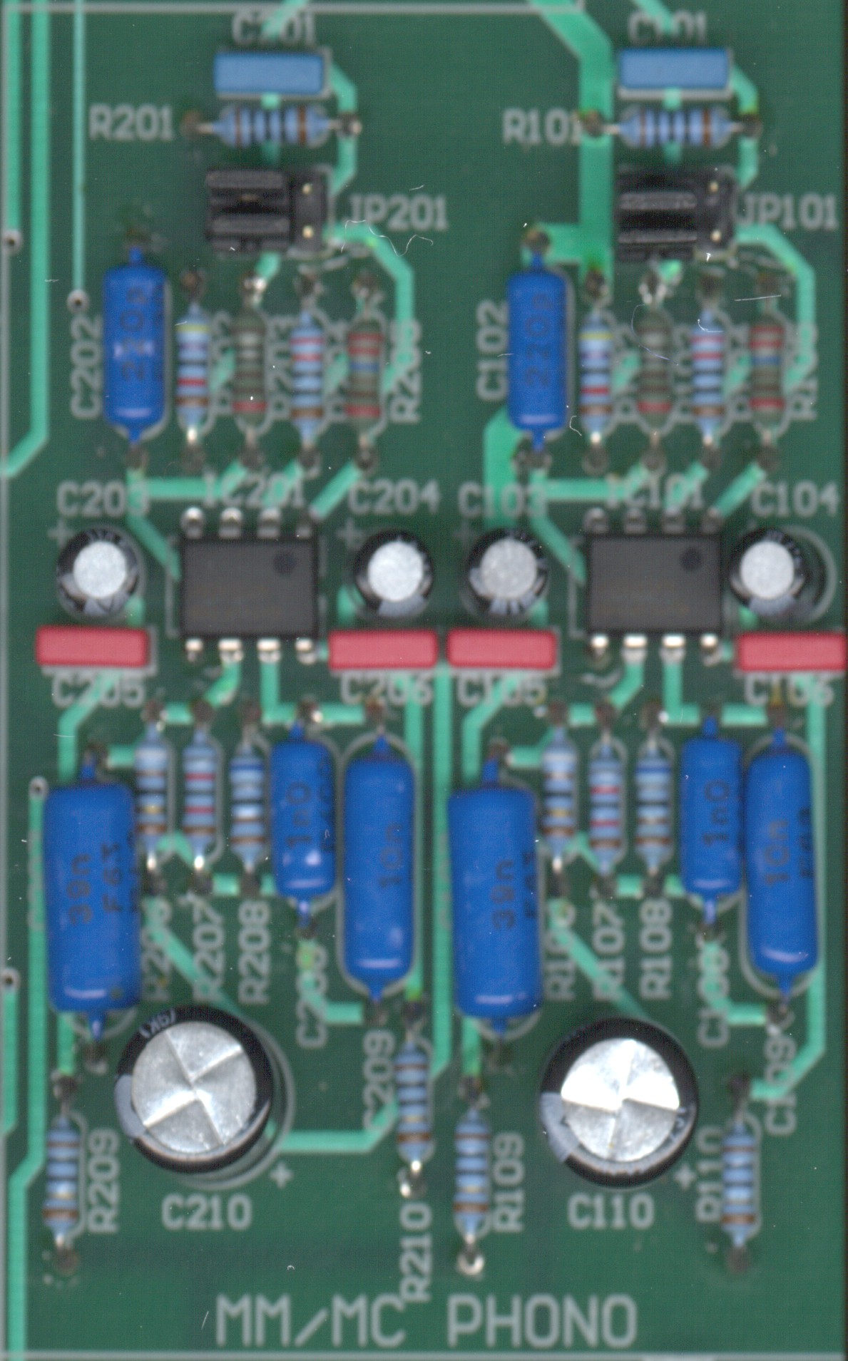 In
the Puccini "remote" there is still the Phono circuit. It is the same
as
in the original version: an NE5532 chip is used for the MC step-up and
for the MM+RIAA equalization.
In
the Puccini "remote" there is still the Phono circuit. It is the same
as
in the original version: an NE5532 chip is used for the MC step-up and
for the MM+RIAA equalization.
After this there are relays for input selection. Then the signal
goes
to the motorized ALPS, and at least to the preamplifier section.
Here we have the first big difference with the original Puccini: the
impedance seen by the inputs is not constant, but vary with the
position
of the volume knob! This happens because there is no "isolation" stage
BEFORE the volume itself, while in the original Puccini there was a
follower
ahead.
It is now time to download the diagram (as usual is a zipped PS, 28k)
This is not the entire Puccini "remote" (it lacks the logic part), but it is detailed enough to understand how it works.
 As
you can see the diagrams start to be different than the original
Puccini
after the volume knob, where the first active stage is the discrete
Op-Amp
previously discussed; the Closed-Loop gain is set to [1+(11500/3320)] =
4.46 times; but due to the insufficient OL gain the real measured value
is near 4 (12dB). DC gain is set to 1, due to the decoupling action of
C118.
As
you can see the diagrams start to be different than the original
Puccini
after the volume knob, where the first active stage is the discrete
Op-Amp
previously discussed; the Closed-Loop gain is set to [1+(11500/3320)] =
4.46 times; but due to the insufficient OL gain the real measured value
is near 4 (12dB). DC gain is set to 1, due to the decoupling action of
C118.
In this circuit (as well as in other part of the "remote") there is
a large use of "audio grade" electrolytic capacitors: the
ELNA Starget.
All the resistors are Welwyn RC55 metal film.
(note that diode D? was forgot in the PCB, and was thus added in series to R120 with a "flying weld")
The power supply is regulated at +/- 15Vdc with two ordinary
7815/7915
ICs; input is taken from the raw DC supply (about +/- 40Vdc), with the
help of a series 390W 5W resistor at the
input;
since the current is 40mA, the voltage at the input of the regulators
will
be about 25Vdc.
Two toroidal transformers are used (200VA each channel), but for the
preamplifier section (ChL and ChR, +/- 15Vdc) the supply is taken only
from the Left Channel transformer.
There is another AC input (the ones devoted to power the logic
part),
derived from a supplementary winding of the ChR toroidal transformer.
Well, nothing much to say about this preamplifier stage; it really
does
its work (apart from the input resistance problem), the bandwidth is
more
than necessary, the gain is adeguate.
On the contrary the power stage is difficult to understand!
Here we have again the same discrete FET stage, in place of the
NE5534 original IC.
All the resistors are changed to higher values in order to be powered
by a +/- 32Vdc supply, obtained with the help of a simple transistor
stabilizer
(made with Q107/Q108 and zener diodes) from DC.
But a detailed look at the currents reveal that the FET input stage is biased with an Id of only 150uA, about five times less than in the preamplifier section.The following pair of transistors are biased with 3.7mA, and the last two at a higher value of 16mA; I suppose this is due to the very difficult load offered by the output power stage (very low, at least near 1kW, and highly non linear).
This brings the problem that the global frequency response of all the Puccini "remote" is not flat (like the old one), but has a -3dB point at about 40kHz, so -1dB at 20kHz and -0.3dB at 10kHz. Talking of phase, this is about 27 degrees of lag at 20kHz and 14 degrees at 10kHz.Not only! All the distortion generated in the high frequencies by the output transistor (e.g. the crossover distortion) will not "killed" by the feed-back.
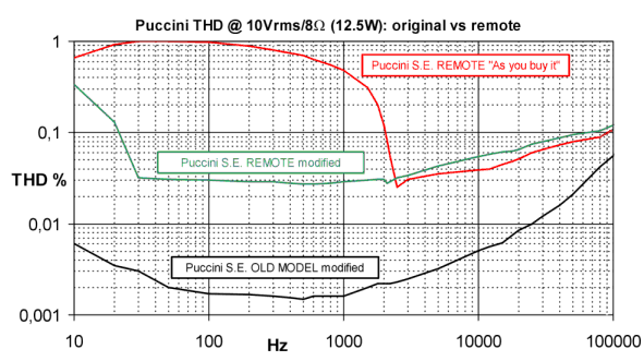
Do you remember the "Errors revealed" section in the Donizetti web page? Well it seems that someone has not read it!Take a look at the Puccini "remote" THD plot, compared with the original Puccini: as you can see the THD value is worse, even with the capacitors changed with the new 10uF value.
In the Puccini "remote" still there are two capacitors (C156/C157) with the wrong value!
This is due to the low Open-Loop gain. The high frequency rise is
due
to the C155 capacitor local feed-back.
Whats left to say?
The declared output power is 60W. It is reached with a 230Vac mains;
no more is possible due to the 32Vdc stabilized supply of the driving
section.
In case of a short circuit there is a current-limiting circuit copied
"as
is" from the
Aida integrated amplifier, even with two "non
sense" resistors (R159/R164); these were used in the original circuit
to
obtain a divider (with other two series resistors), reducing the
sensitivity
of the limiter.
In the "remote" circuit the value of R160/R163 has been increased,
lowering the maximum frequency the circuit will still work (see it as a
low pass filter, made with R163 + C159). So doing only a "steady-state
screwdriver short circuit" allows Q115/Q116 to conduct.
At the same time the photocoupler IC103 pulls down a pin of the
microcontroller,
opening all the relays and stopping the music.
Nothing happens in case of voltage clipping.
I'm not sure, but it seems to me that there is no DC sensing of the
output. In case of transistor failure (short circuit), a DC current
will
flow through the speakers; what if the fuses don't blow?
That's all, folks.