
Nessun dorma!... Nessun dorma!...
Tu pure, o Principessa,
nella tua fredda stanza
guardi le stelle che tremano...
d'amore e di speranza!
Ma il mio mistero è chiuso in me,
il nome mio nessun saprà!
No, no, sulla tua bocca lo dirò,
quando la luce splenderà!
Ed il mio bacio scioglierà
il silenzio che ti fa mia!
(Il nome suo nessun saprà...)
(E noi dovrem ahimè, morir, morir...)
Dilegua, o notte! tramontate, stelle!
Tramontate, stelle! All'alba vincerò!
Vincerò! Vincerò!
Puccini integrated amplifier
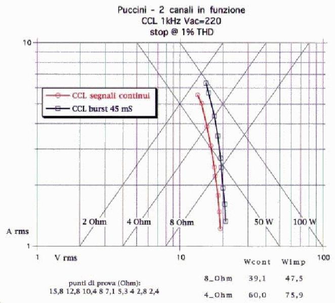 Voltage
and Current in a bi-logarithmic plane
Voltage
and Current in a bi-logarithmic plane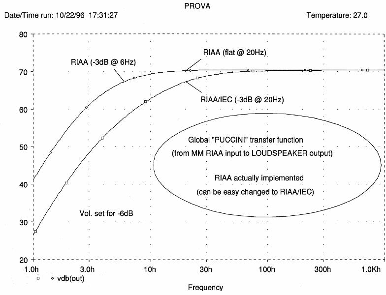 If
you want to implement the RIAA/IEC curve (-3dB@20Hz), change C2 to
100uF.
If
you want to implement the RIAA/IEC curve (-3dB@20Hz), change C2 to
100uF.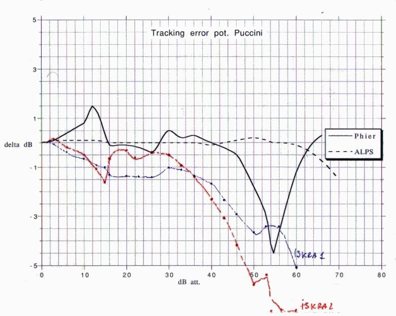 It could be a good
idea to have a look inside your Puccini: is the pot an ALPS ?
It could be a good
idea to have a look inside your Puccini: is the pot an ALPS ? This
is the FIRST prototype of Puccini, presented to the WCES 1996.
This
is the FIRST prototype of Puccini, presented to the WCES 1996. THD
vs Frequency param. Load; not too bad at all.
THD
vs Frequency param. Load; not too bad at all.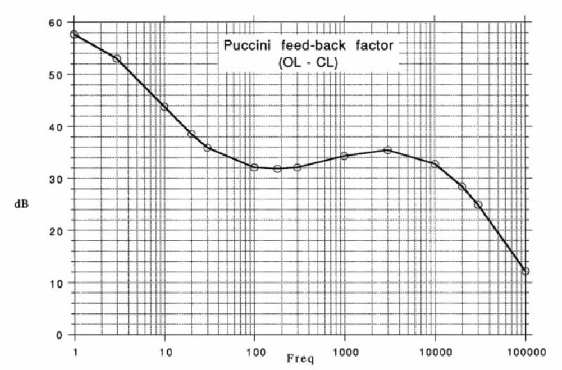 This is a PSpice
simulation of the Feedback factor, not a measured one !
This is a PSpice
simulation of the Feedback factor, not a measured one !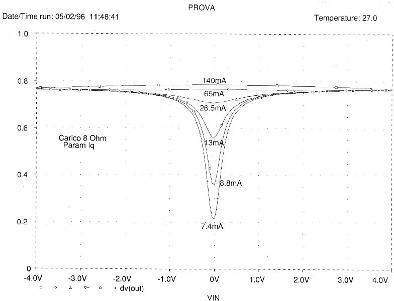 The
20mA idle current is a good compromise for the Puccini
The
20mA idle current is a good compromise for the Puccini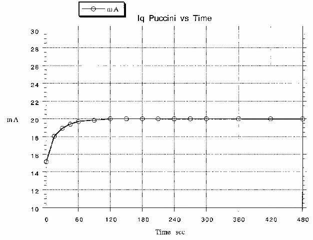 The
thermal feedback has a set-up time of about one minute, as is visible
in this test
The
thermal feedback has a set-up time of about one minute, as is visible
in this test